
When choosing a TVS diode for a 24 V industrial power supply, a buyer may start with three requirements: surface mounting, a 600 W rating and an acceptable price. The more important question is what voltage the downstream chip will actually see during a surge.
DOWOSEMI's P6SMB series provides a useful example. Its peak pulse-power rating describes the stress the device can withstand under specified conditions. Whether it protects a particular circuit is a separate question.
1. What does the 600 W rating mean?
A TVS normally carries only a small leakage current. During an overvoltage transient, it conducts and diverts surge current, limiting the voltage across the protected node.
P6SMB devices use the SMB, or DO-214AA, surface-mount package. The stated 600 W is peak pulse power for a 10/1000 μs waveform, with a reference ambient temperature of 25°C. The datasheet also specifies conditions such as a non-repetitive pulse, mounting copper and temperature derating.
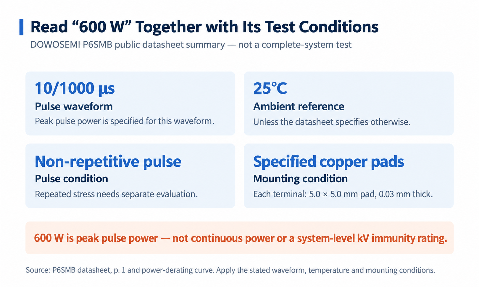
Figure 1. Conditions accompanying the P6SMB peak pulse-power rating, summarized from the public datasheet. This is not a complete-system surge-test result.
It is not a continuous 600 W power rating. Nor does it establish that a complete product will pass a particular kilovolt-level surge test. A component's pulse rating and a system's immunity level describe different things.
The waveform matters as much as the headline power. Ratings for a 10/1000 μs pulse and an 8/20 μs pulse cannot be compared directly. Pulse duration, current and temperature change the stress on the TVS. Define the transient expected at the port and the voltage limit of the downstream circuit before selecting the device.
2. Check standoff, breakdown and clamping voltage separately
Three voltage parameters have different jobs:
- VRWM, reverse standoff voltage: the voltage used to specify normal-operation leakage behavior.
- VBR, breakdown voltage: the voltage measured at a specified test current.
- VC, clamping voltage: the voltage across the TVS at a specified peak pulse current.
Normal operation calls for a suitable VRWM. Protection calls for a suitable VC under the relevant stress. VBR cannot stand in for either check.
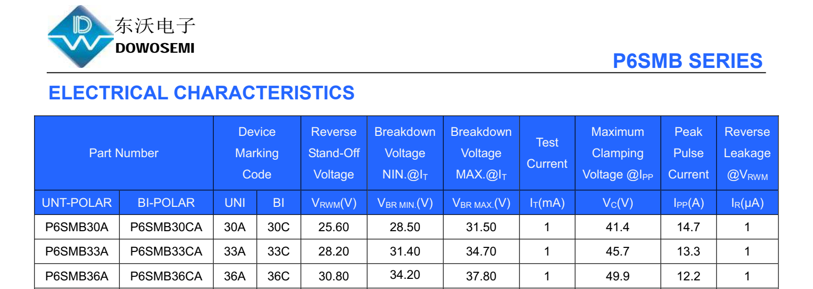
Figure 2. Original manufacturer table, excerpted from page 3 and checked on September 14, 2026. Read VC together with IPP in the same row. The part-number voltage grade is not the reverse standoff voltage. The manufacturer's brand mark is retained.
The table gives the following values for the unidirectional A versions:
| Part | VRWM | Maximum VC | Specified peak pulse current |
|---|---|---|---|
| P6SMB30A | 25.6 V | 41.4 V | 14.7 A |
| P6SMB33A | 28.2 V | 45.7 V | 13.3 A |
| P6SMB36A | 30.8 V | 49.9 V | 12.2 A |
The “30”, “33” and “36” in these part numbers should therefore not be read as 30 V, 33 V and 36 V standoff ratings.
Consider a hypothetical 24 V supply with a ±10% tolerance and a downstream chip with a 40 V absolute maximum rating. This is a teaching example, not a verified customer circuit.
The supply may reach 26.4 V in normal operation. P6SMB30A has a VRWM of only 25.6 V, so it does not cover that upper supply limit under its specified standoff condition. A higher breakdown voltage does not resolve this mismatch.
P6SMB33A, with a 28.2 V standoff voltage, clears the 26.4 V supply limit. But its maximum specified clamping voltage is 45.7 V, above the hypothetical chip's 40 V absolute maximum. Selecting it solely because its standoff voltage is high enough does not establish protection.
This does not mean P6SMB33A is unsuitable for every 24 V system. The 45.7 V value is specified at 13.3 A; the actual surge current depends on the waveform, source impedance and circuit. The relevant question is whether the downstream pin stays below its allowable voltage with adequate margin under the defined test conditions. An absolute maximum rating is not a normal operating target.
The three rows also specify different pulse currents. They are not a same-current clamping comparison. If the available window between the maximum normal supply voltage and the downstream limit is too narrow, revisit the clamp, the downstream device or the protection architecture. Moving to a higher TVS voltage grade alone may make clamping worse.
3. Temperature, hot-plugging and repeated stress change the problem
A supply input may experience more than a standardized external surge. Cable inductance can create an overvoltage when a DC adapter is connected. ROHM's public application material illustrates this hot-plugging mechanism and the role of input protection.
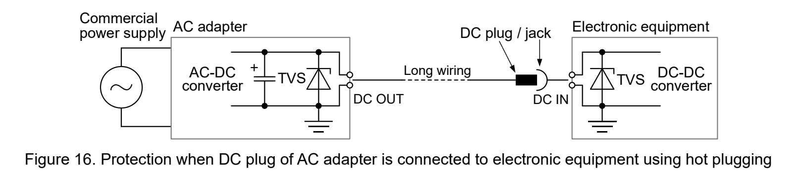
Figure 3. Original ROHM application illustration, ©2023 ROHM. It explains a protection mechanism; it is not evidence of a DOWOSEMI customer design or an approved bill of materials.
A 25°C rating cannot simply be carried over to a hot enclosure. Follow the manufacturer's derating curve and its stated temperature reference, mounting conditions and pulse conditions. Checking only the maximum junction temperature is insufficient.
Single-pulse capability, repetitive-transient capability and sustained-overvoltage behavior are also different requirements. Passing one pulse does not establish survival under repeated events with limited cooling time. Repetitive stress needs its own evaluation.
For a sustained abnormal input, protection may need coordinated current limiting, a fuse or an active disconnect. A higher TVS pulse-power rating does not replace analysis of where the continuing fault energy will go.
4. Verify the protected pin, not just the TVS
PCB traces, vias and return paths add parasitic impedance. Consequently, the voltage at the downstream chip can differ from the voltage measured directly across the TVS. Layout is part of the protection design.
A useful validation checks the protected pin's waveform, circuit operation, recovery after the event and any relevant post-test parameter changes. “The TVS did not fail” is not, by itself, evidence that the downstream circuit was adequately protected.
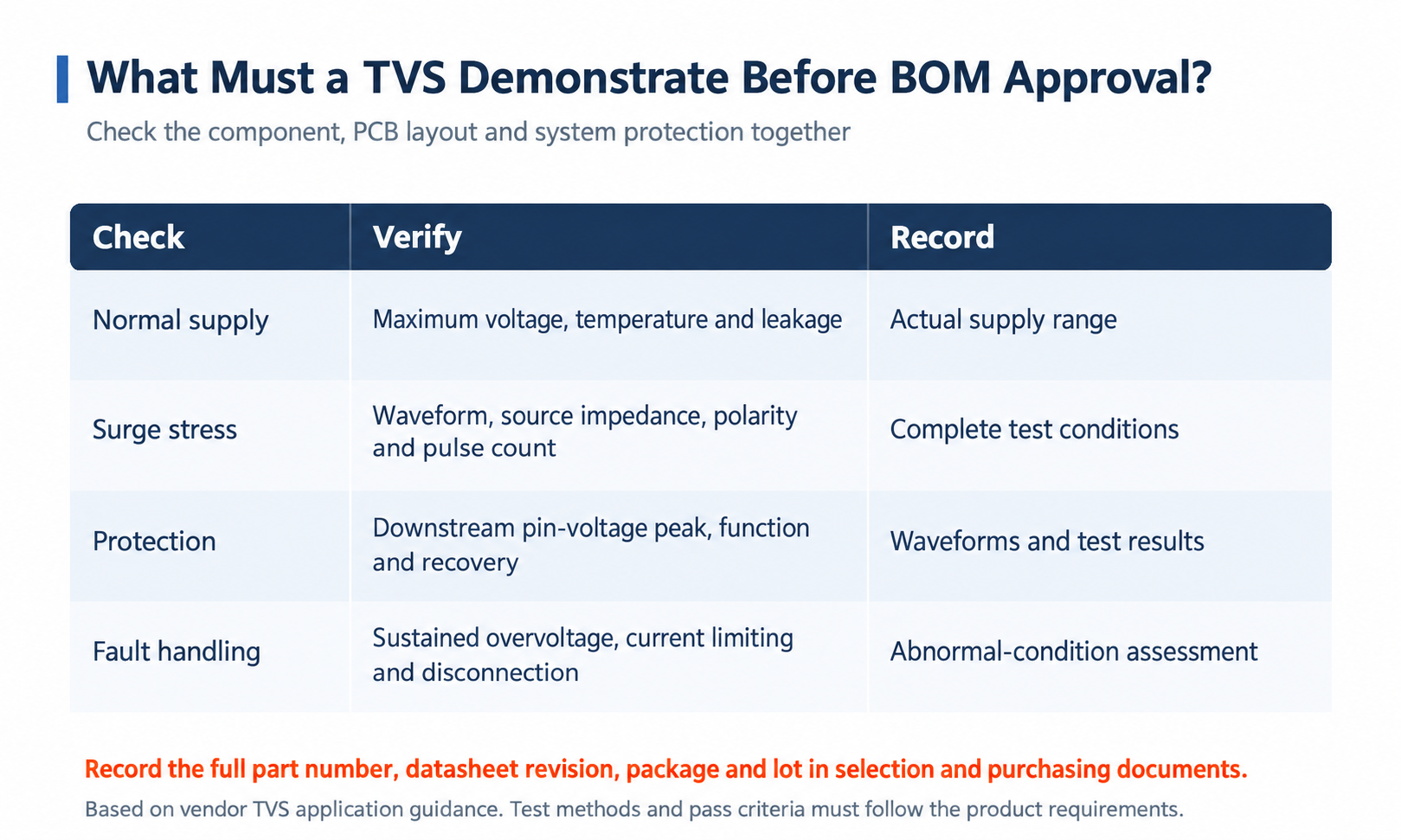
Figure 4. Suggested checks and records before adding the selected TVS to the BOM. Test methods and acceptance criteria must follow the product's requirements.
Record the waveform, source impedance, polarity, number of pulses, temperature and supply operating state. A result without those conditions is difficult to reproduce or apply to another design.
Purchasing and engineering records should identify the complete part number, suffix, package, datasheet revision and lot. A vendor test report is useful only when the tested part, circuit and conditions match the intended application closely enough. A successful test on a different board is not a substitute for testing this board.
Maintain traceability and decide when changes in component lot, layout or specifications require revalidation. The selected rating belongs in a documented protection design, not just in a purchasing description.
Conclusion
A 600 W rating is a first screening criterion for a 24 V power-supply TVS. A sound choice must satisfy normal-operation leakage and voltage requirements, clamp the protected node within its limits, and withstand the specified electrical and thermal stress.
Tie those requirements to the BOM and to reproducible verification. That is what turns a pulse-power label into evidence of circuit protection.
This article uses illustrative cases and public manufacturer documentation. Final selection must follow the applicable vendor specifications and complete-system testing; the examples do not constitute a verified customer design.