
Demand for compute has not yet satisfied the AI chip market, but the upstream substrate industry is already running short. Recent market forecasts put the ABF substrate supply-demand gap at 20%-40%, while visibility from orders and long-term agreements for some advanced capacity extends into 2027-2028. At first glance, this looks like another expansion story in which any factory can profit: Ajinomoto adds ABF film; Ibiden, Unimicron, Nanya PCB, and Kinsus expand advanced substrates; SCC and Fastprint accelerate FC-BGA projects; and the shortage disappears as equipment moves into new buildings.
The counterintuitive reality is that the industry is short not merely of floor space or rolls of ABF film, but of effective advanced capacity that has passed material, process, packaging, and customer qualification. Even after a line is powered on, stable deliveries may still require two rounds of yield ramp, three rounds of reliability testing, and a customer-qualification clock that can restart at any time.
1. A Forecast Gap of 40% Does Not Mean Every ABF Substrate Is in Shortage
The 20%-40% claim needs context. One aggressive market scenario projects an approximately 10% gap for advanced ABF substrates in the second half of 2026, widening to about 21% in 2027 and potentially 42% in 2028. These figures are forward-looking institutional estimates, not an audited inventory count for the entire industry today. They cannot be translated directly into "all ABF substrates are 40% short." The genuine constraint is large-format, high-layer-count, high-routing-density FC-BGA substrates for AI servers, high-performance CPUs, GPUs, and custom ASICs. Mature specifications used in conventional PCs and consumer electronics may not share the same demand or utilization profile.
Similarly, "orders extending into 2027-2028" is more accurately a statement that visibility, customer reservations, and long-term agreements for advanced capacity extend into those years. It does not mean every line at every substrate producer is fully committed. One strong signal is Ibiden's 2026 announcement that it planned to invest about JPY 500 billion in its electronics business during fiscal 2026-2028, including roughly JPY 220 billion in the first phase for additional high-performance IC package-substrate capacity, with sequential mass production planned from fiscal 2027. A long-established leader making that commitment supports the reality of advanced demand. The fact that new capacity arrives only from 2027 also shows that today's shortage has no instant expansion switch.
2. Ajinomoto Does Not Supply Just a Film, but a Material-Process Recipe
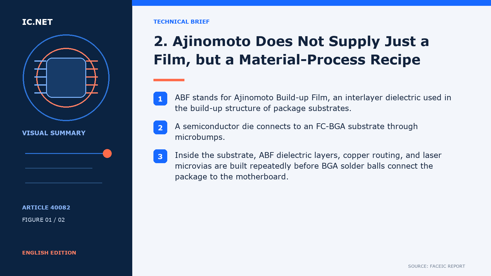
ABF stands for Ajinomoto Build-up Film, an interlayer dielectric used in the build-up structure of package substrates. A semiconductor die connects to an FC-BGA substrate through microbumps. Inside the substrate, ABF dielectric layers, copper routing, and laser microvias are built repeatedly before BGA solder balls connect the package to the motherboard. ABF film is not an ABF substrate, and it is not electronic plastic wrap that can simply be applied before shipment. It must meet requirements for insulation, low thermal expansion, laser via formation, direct copper plating, adhesion, and heat resistance. A change in material grade or generation can force renewed work on laser parameters, plating windows, line and space, warpage, and reliability data.
Ajinomoto states that ABF became a de facto standard for high-performance CPU substrates after a major semiconductor manufacturer first adopted it in 1999. In May 2026, the company announced a third ABF production site in Gifu, scheduled to begin construction in 2028 and production in 2032, explicitly addressing demand beyond 2030. The project confirms that the material side still needs more capacity, but it also exposes an overly optimistic narrative: a factory entering production in 2032 cannot solve deliveries in 2026-2028. Supply over the next two years will depend more heavily on capacity adjustments and scheduling at the existing Kawasaki and Gunma sites, together with the efficiency of matching each ABF generation to substrate processes.
3. The Factory Is Nearly Complete, So Why Has Customer Qualification Not Turned Green?
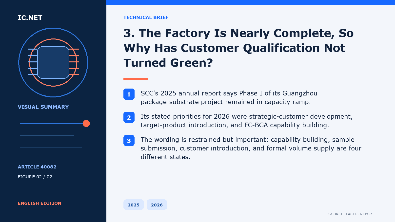
China does have FC-BGA projects. SCC's 2025 annual report says Phase I of its Guangzhou package-substrate project remained in capacity ramp. Its stated priorities for 2026 were strategic-customer development, target-product introduction, and FC-BGA capability building. The wording is restrained but important: capability building, sample submission, customer introduction, and formal volume supply are four different states. Without public disclosure of a specific customer and a stable volume relationship, market speculation cannot fill in the missing step for the company.
Fastprint's project progress illustrates the issue even more clearly. Its 2025 annual report gave the Guangzhou FCBGA project a budget of RMB 5 billion and year-end construction progress of 63.41%. The Zhuhai FCBGA project had a budget of RMB 1 billion and was 91.72% complete. The same report, however, disclosed an impairment on the Zhuhai project because "mass-production progress and investment returns fell short of expectations," and the project was transferred to fixed assets during the year. In other words, 91.72% construction progress is not 91.72% yield, and it certainly does not mean customer qualification is complete. For an advanced substrate, completion of the building is the starting gun. Fine-line patterning, laser microvias, plating uniformity, layer-to-layer registration, warpage control, thermal cycling, and lot consistency still have to be mastered.
4. Domestic Substitution Fails When the Word “Domestic” Is Used to Skip BOM Validation
Sourcing an ABF substrate cannot be reduced to asking whether a domestic option exists or comparing unit prices. The specification needs to lock package dimensions, substrate layer count, line and space, microvia structure, cored or coreless construction, warpage limits, surface finish, test coupons, the designated generation of ABF material, and the approved-material list. In AI and HPC products, larger area, more layers, and higher power simultaneously amplify warpage, thermal stress, and yield risk. A nameplate capacity of 100 square meters may ultimately deliver far less than 100 square meters of qualified area.
A more realistic domestic-adoption path starts with domestic CPUs, networking chips, and specialized ASICs that have fewer layers, smaller package dimensions, and manageable platform risk. The material supplier, substrate producer, OSAT, and chip-design company should validate the stack jointly from the beginning of a new project. The incumbent supply plan should remain available until volume production, rather than treating a single material change as qualification-free. After material matching, the program must still pass substrate prototyping, package assembly, reliability validation, customer or platform qualification, and finally stable volume delivery. A vendor on an evaluation list can only be described as under evaluation. A completed sample submission can only be described as sampling. Without formal disclosure, neither can be called an active supplier.
Conclusion: the Scarce Resource Is Not ABF Film, but Qualified Area
The expected ABF substrate tightness of 2026-2028 is structural. Mature specifications may remain available, while large-format, high-layer-count, low-warpage products for advanced AI and HPC could become tighter even as companies expand. Any delay in Ajinomoto's material capability, the advanced processes of leaders such as Ibiden, a substrate maker's yield ramp, or customer qualification can turn nameplate capacity into capacity that exists but cannot be used.
For sourcing teams, three harsher indicators matter more than expansion headlines: whether the exact specification has completed customer qualification, whether yield is stable across lots, and whether critical materials have approved dual sources. The decisive measure for domestic FC-BGA will not be how quickly a factory photograph appears, but who can repeatedly deliver each square meter of substrate that a customer is willing to mount a chip on.
Disclaimer: This article is for industry information exchange only. It does not constitute investment advice, part recommendations, or a judgment about any unconfirmed supply relationship.