
If an AI server were a kitchen, HBM would be the worktop beside the chef: fast and immediately accessible, but limited in area. An SSD would be the basement store: spacious, but every ingredient takes longer to retrieve.
As models grow and context windows lengthen, the question becomes unavoidable: where does data go when HBM is full? Adding more HBM increases cost, power, and packaging pressure. Sending data back to SSD can leave the GPU waiting for delivery.
Could another shelf fit between HBM and SSD?
In August 2026, SK hynix and Sandisk published the first open HBF specification. HBF, or High Bandwidth Flash, seeks to use NAND's high capacity and nonvolatility to create a storage tier closer to the GPU than an SSD but below HBM.
It sounds like the standard answer—faster, larger, and cheaper at once. Storage is rarely so accommodating. The most important question is not whether HBF can replace HBM, but whether it can keep some data from having to occupy HBM at all.
01. The Specification Is Public, So Why Can No One Buy HBF Yet?
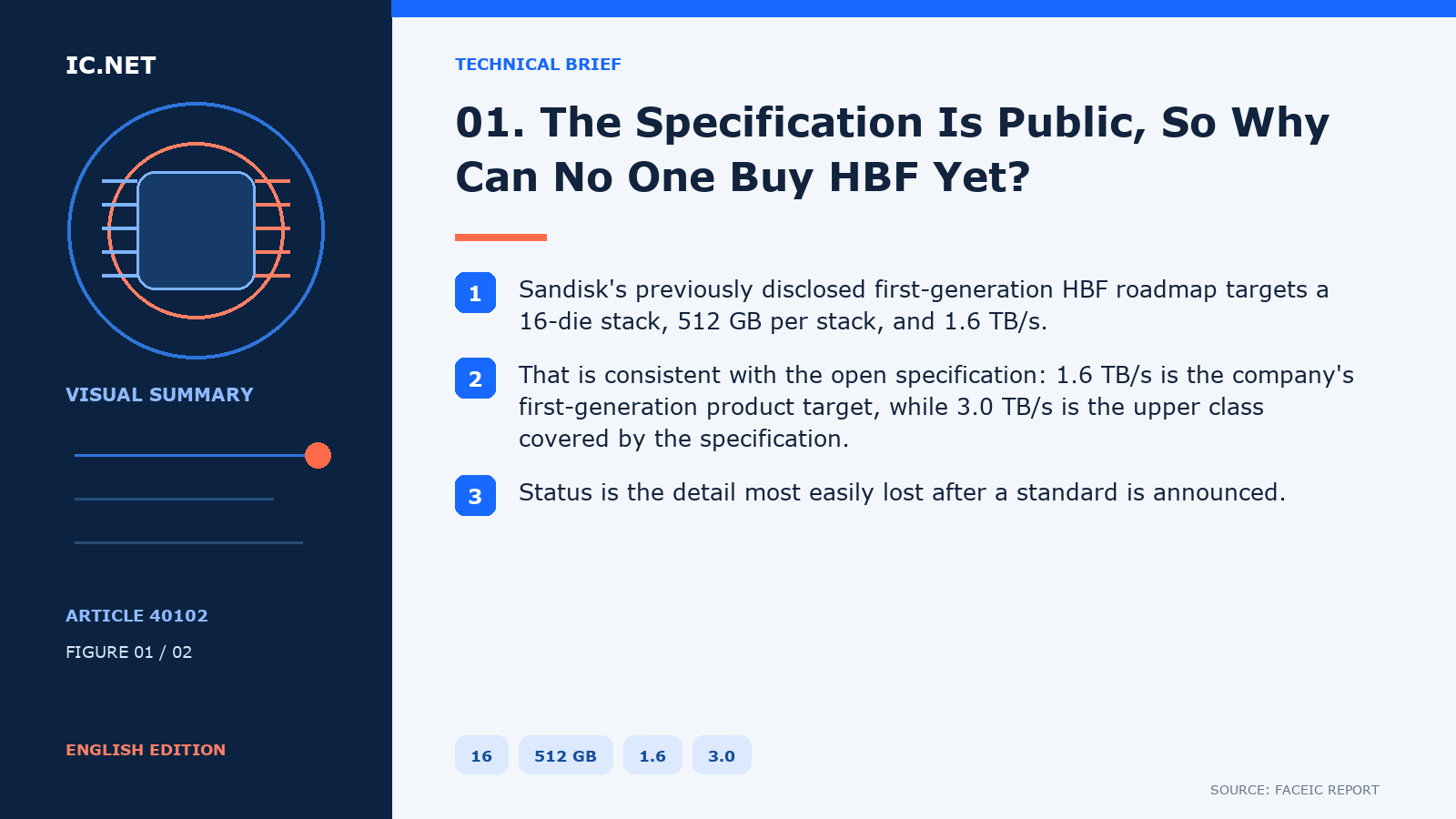
The first HBF specification supports stacks of 8 or 16 NAND dies, with capacity up to 512 GB per stack and three bandwidth classes spanning approximately 0.4 TB/s to 3.0 TB/s. It is designed to connect to a CPU or GPU through UCIe, and the specification also covers the electrical interface, reliability, packaging, and software I/O.
The headline 3.0 TB/s may tempt some observers to declare that flash has caught HBM. That would be premature. The 0.4-3.0 TB/s range covers three specification classes. It does not mean every HBF device reaches 3.0 TB/s, and it does not establish the existence of a production 512 GB, 3.0 TB/s product available to buyers.
Sandisk's previously disclosed first-generation HBF roadmap targets a 16-die stack, 512 GB per stack, and 1.6 TB/s. That is consistent with the open specification: 1.6 TB/s is the company's first-generation product target, while 3.0 TB/s is the upper class covered by the specification.
Status is the detail most easily lost after a standard is announced. HBF is currently being advanced as an open standard through OCP. It is not a mature JEDEC standard that every memory producer can already implement. Sandisk previously targeted initial samples for the second half of 2026 and samples of HBF-equipped AI inference devices for early 2027.
Can HBF be described today as being in mass production? No. Publishing the specification is equivalent to releasing construction drawings. Samples, controllers, packaging, software, and customer qualification still stand between those drawings and a store opening for business.
02. Is a Tier Really Missing Between HBM and SSD, and What Belongs in HBF?
AI inference repeatedly reads model weights, while long-context applications produce an expanding KV cache. HBM's high speed and low latency make it suitable for the hottest and most frequently accessed data. SSDs provide far more capacity, but their distance from the compute unit, bandwidth, and access path prevent them from behaving like GPU memory.
HBF moves NAND flash closer to the processor and uses a high-bandwidth interface to reduce data movement. NAND retains data without power, so model weights could be stored in HBF in advance instead of being reloaded from SSD whenever a system starts, loads a model, or switches models.
The best early candidates are likely model weights, cold expert modules, and frequently read but infrequently modified data. They resemble reference books in a library: consulted often, but not rewritten every minute.
Does KV cache belong there too? That cannot be assumed. KV cache grows and is written continuously with context, while NAND has asymmetric read and write behavior, write-granularity constraints, endurance limits, and latency. Some research models therefore prioritize HBF for relatively static model weights rather than large volumes of dynamic KV cache.
HBF's most realistic early role may not be universal memory, but a very large, predominantly read-only near-storage tier. Put every kind of data into it and the new architecture may quickly become a new bottleneck.
03. A 1.6 TB/s Target and a 2.2% Performance Gap Sound Impressive—Are They Production Measurements?
Sandisk has described an internal simulation using 8-bit weights for the Llama 3.1 405B model. In its disclosed result, a system using HBF stayed within 2.2% of the performance of an "HBM system without capacity constraints."
That figure attracts attention, but it does not show that HBF can replace HBM at lower cost with only a 2.2% penalty. It is a vendor simulation, not a test of production HBF silicon in a real server. It covers one model, one precision, and a read-intensive weights workload, and the baseline assumes HBM without capacity constraints. A different workload, controller, prefetch policy, or write ratio could change the outcome.
The practical questions are extensive. What is random-access latency? What write bandwidth and endurance are available? How are bad blocks managed? Where does ECC reside? Who provides the controller? How does a GPU identify the tier? When does software move data from SSD to HBF and then from HBF into HBM?
UCIe can address part of the chiplet-interconnect problem, but it only builds the road to the door. A road does not operate the logistics system. HBF's experience will be determined by the controller, prefetch algorithms, memory-tiering software, and inference framework working together.
Buyers also cannot compare only cost per gigabyte. HBF adds a logic base die, packaging, a controller, and software-integration cost. It may change accelerator package area, cooling, and test. Without production samples and system measurements, it is too early to know whether the HBM cost saved will exceed the added system cost.
04. China Has Three Pieces of the Puzzle, but Not Yet an HBF Supply Chain
HBF is not ordinary NAND with a different interface. It requires high-density NAND die, a logic base die, wafer bonding or TSV stacking, advanced packaging, UCIe, a controller, and a software ecosystem. Chinese companies possess parts of that stack, but separate puzzle pieces do not constitute a finished product.
YMTC's Xtacking 4.0 fabricates the memory array and peripheral circuitry separately before wafer bonding. Public products include the 1 Tb TLC X4-9070 and 2 Tb QLC X4-6080. That shows a domestic technology base in high-density NAND and wafer bonding. The devices remain NAND products and cannot simply be relabeled as domestic HBF.
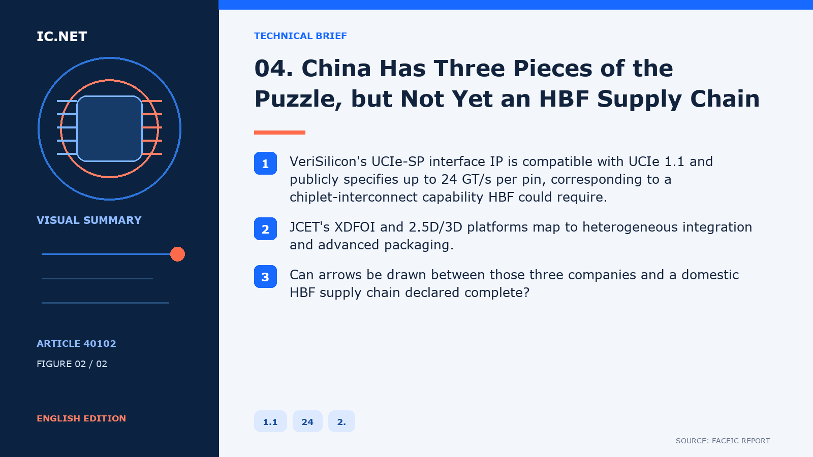
VeriSilicon's UCIe-SP interface IP is compatible with UCIe 1.1 and publicly specifies up to 24 GT/s per pin, corresponding to a chiplet-interconnect capability HBF could require. JCET's XDFOI and 2.5D/3D platforms map to heterogeneous integration and advanced packaging.
Can arrows be drawn between those three companies and a domestic HBF supply chain declared complete? No. Public information does not show that they have formed a formal HBF alliance, introduced an end-to-end product, or entered the volume BOM of an AI accelerator customer.
Before domestic HBF becomes real, it still needs a common interface, a sample platform, bandwidth and endurance testing, package thermal validation, controller integration, software tiering, and system-customer qualification. Domestic substitution is not only a question of which puzzle piece is missing. Someone has to assemble all the pieces into a machine that can operate continuously.
Conclusion: Will HBF Displace HBM, or First Become Its Capacity Partner?
HBF has appeared because AI inference datasets are growing and keeping all data permanently in HBM increasingly resembles using premium city-center property as a warehouse. Putting everything on SSD is like locking the chef's seasonings three floors underground.
HBF proposes a larger shelf near the processor. The hottest data stays in HBM; read-intensive model weights and cold data move into HBF; and long-term data remains on SSD. The three form a hierarchy rather than eliminating one another.
The next milestones are not additional roadmap slides, but testable samples, support from mainstream CPUs or GPUs, measured bandwidth and latency, endurance under real workloads, and system economics that improve on simply adding more HBM.
Publication of the HBF specification is only the starting signal. Whether HBF earns a new place in the AI inference BOM will ultimately be decided jointly by chips, packaging, software, and customers.
Disclaimer: This article analyzes public information and does not constitute investment, procurement, or part recommendations. Product parameters, production status, and supply relationships are subject to the latest formal disclosures from the manufacturers.