
Small inductors in AI servers are attracting a substantial investment.
On September 14, MoneyDJ, citing Nikkei, reported that TDK planned to invest a total of ¥40 billion in two Japanese plants to expand thin-film inductor production for AI semiconductors and optical transceivers. The amounts and plant allocations are media-reported plans. TDK had already stated in its official earnings presentation that it would accelerate thin-film inductor capacity expansion.
Behind the investment are two different circuit requirements. Processor power delivery must limit losses along high-current paths. Optical-transceiver bias circuits must supply DC while isolating signals. Both use inductors, but their performance tradeoffs differ substantially.
1. Two plants, two application requirements
According to the report, ¥35 billion would go to the Kofu plant in Yamanashi Prefecture for thin-film inductors used with AI semiconductors, and ¥5 billion to the Tsuruoka East plant in Yamagata Prefecture for optical-transceiver inductors.
The planned Kofu investment is seven times the Tsuruoka East amount. That does not establish a seven-to-one ratio in capacity, sales or market size: the report provides neither product quantities nor the cost of a unit of production capacity.
In its April 2026 earnings presentation, TDK identified low-voltage, high-current vertical power delivery, together with thin-film inductors and chip beads for optical transceivers, as AI-related opportunities. It also discussed bringing forward inductor expansion based on thin-film technology developed for HDD magnetic heads.
The shared thread is manufacturing experience. It does not make the specifications of the two product groups interchangeable. A miniature optical-transceiver bias inductor cannot be used as evidence of processor power-delivery capability.
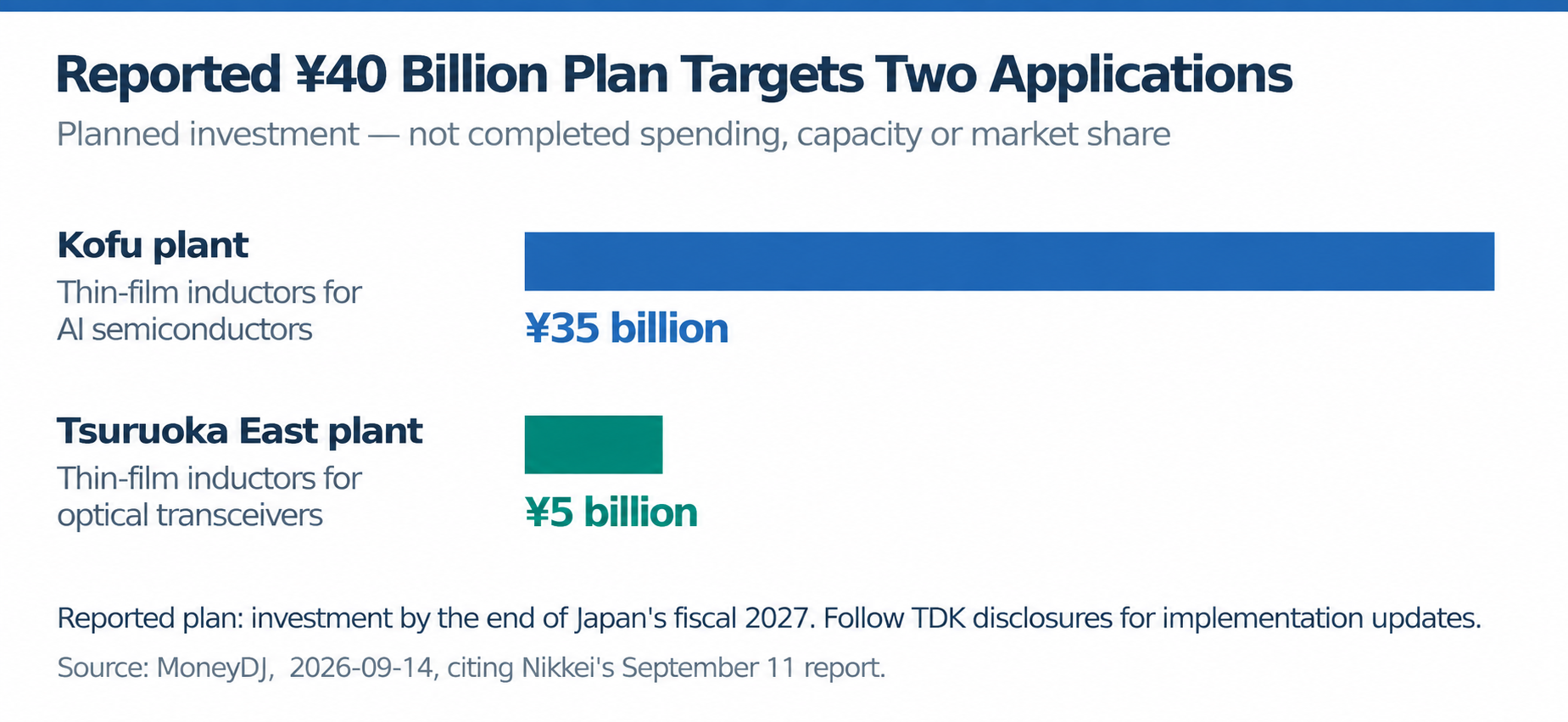
Figure 1. Investment plans as reported by MoneyDJ, not completed investment or capacity figures.
2. Processor power: low voltage makes path losses more costly
Processor power delivery combines increasing power with low operating voltage. Since power equals voltage multiplied by current, supplying more power at the same voltage requires more current. Voltage drop along a resistive path rises as I × R, while resistive loss rises as I²R. Doubling current therefore quadruples heat dissipation in the same resistance.
Consider a hypothetical calculation. At 200 A through 0.1 mΩ, the drop is 20 mV and the loss 4 W. At 400 A, they become 40 mV and 16 W. If the target load voltage is 0.8 V, the latter drop is 5% of that target. Remote sensing can help compensate for steady-state voltage drop, but it does not eliminate the 16 W of path heating. These are illustrative assumptions, not measured TDK product results.
Vertical power delivery aims to place the point-of-load converter on the PCB's reverse side beneath the processor, shortening the board-level high-current path. TDK's FS1525, announced in February 2026, illustrates this approach: the module provides 25 A, is 3.82 mm high, and integrates functions including the power inductor, MOSFETs and control. It shows why placement, component height and cooling need to be designed together. It does not establish that its internal inductor is one of the products covered by the reported expansion.
Thin-film describes a manufacturing process; low-profile describes package height. They are not interchangeable terms. A low-profile inductor that meets the electrical and thermal requirements can enable shorter power routing. But if additional component loss offsets the reduction in path loss, the complete power chain may gain no efficiency. Thickness, current capability and loss must be balanced within the same design.
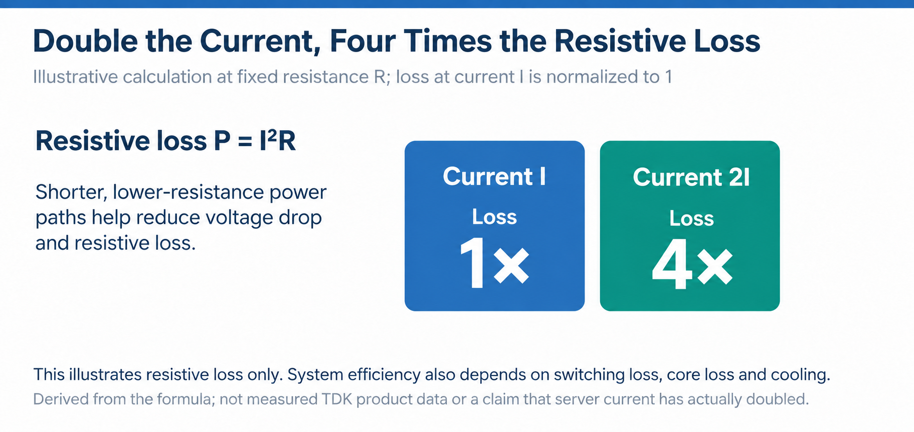
Figure 2. A formula-based illustration, not measurements of a TDK product or server.
3. Optical-transceiver bias circuits: pass DC and isolate signals
A bias tee has a common path carrying both DC and signal. A capacitor blocks DC in the signal branch. The inductor branch supplies DC while impeding signals in the target frequency band from entering the supply. This is among the intended applications of TDK's PLEC69B series, announced in August 2025.
The PLEC69BCA100M-1PT00 has a nominal inductance of 10 μH at 1 MHz, with ±20% tolerance. Its current specifications need especially careful reading. In the datasheet columns labeled “max.”, Isat is 0.20 A for a 30% inductance reduction, and Itemp is 0.35 A for a 40°C temperature rise. The corresponding typical values are 0.25 A and 0.40 A. The manufacturer defines rated current as the smaller of Isat and Itemp.
Using those two “max.” columns gives a 0.20 A rated current, not the thermal column's 0.35 A. This is the manufacturer's selection rule; it does not mean every device loses exactly 30% of its inductance at 0.20 A. If the circuit permits less inductance change, determine the usable current from the DC-bias characteristics and operating temperature. Relying only on the higher temperature-rise current can overstate the ability to retain the required inductance.
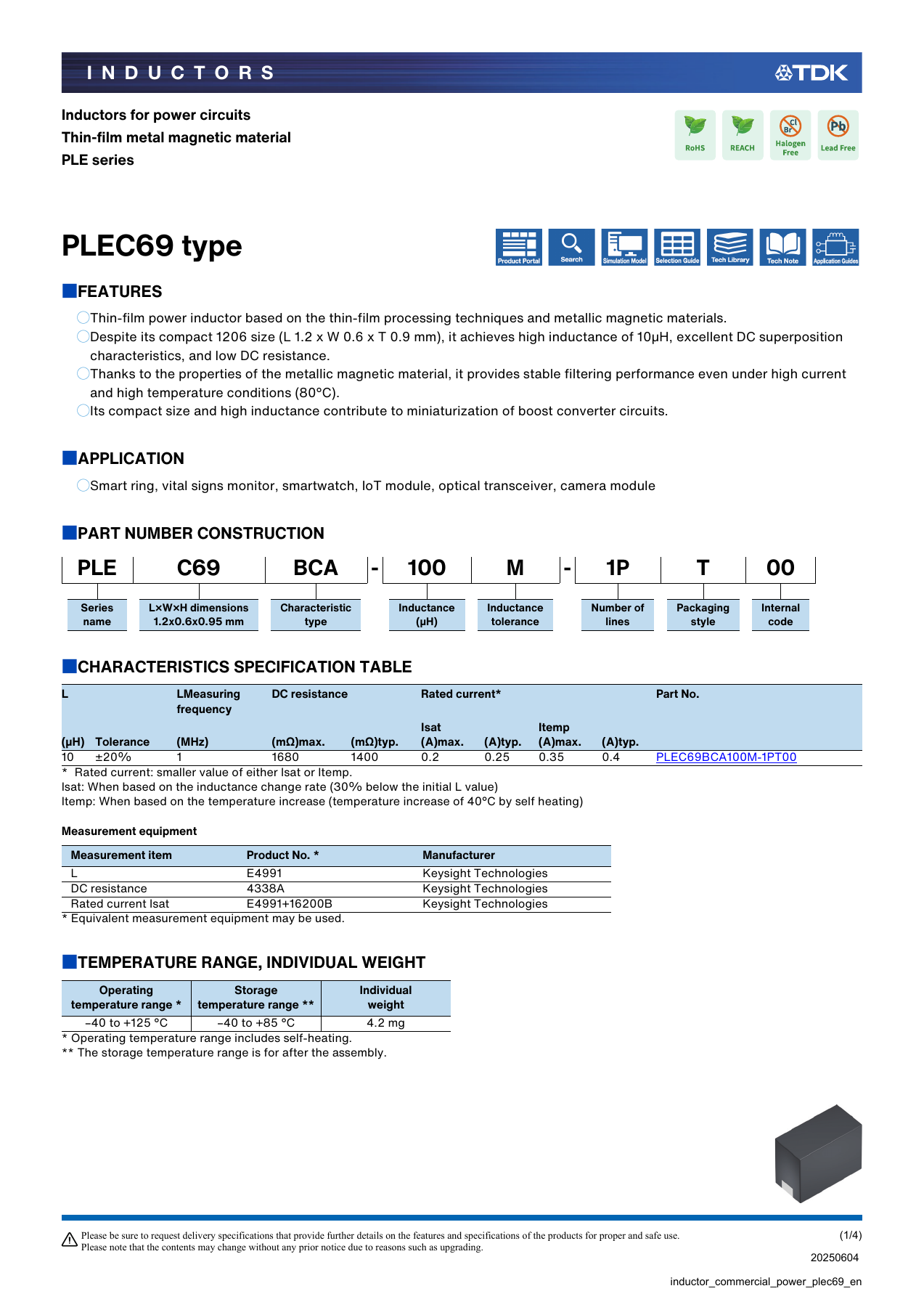
Figure 3. Original TDK datasheet, June 2025 version hosted by Mouser. The cited parameters were cross-checked against TDK's product page and August 26, 2025 announcement.
DC resistance also affects the bias path. With the device's 1.4 Ω typical resistance and an assumed 0.20 A DC current, the calculated drop is approximately 0.28 V, and resistive loss approximately 56 mW. This calculation excludes temperature changes and AC losses, but shows that even a small inductor consumes bias-voltage and thermal margin.
Signal isolation requires a different set of characteristics. TDK's emphasis on high impedance over 10–200 MHz describes how the device impedes signals entering the supply branch in that frequency range. It cannot be converted into an 800G or 1.6T transmission-rate rating. Real inductors also have parasitic capacitance and self-resonance; impedance does not increase indefinitely according to the ideal-inductor equation. A single nominal “10 μH” value therefore cannot fully describe broadband isolation.
The same device needs low DC resistance and high impedance in the target signal band. The former limits bias drop and heating; the latter provides isolation. DC bias also changes the inductor's behavior. These requirements differ markedly from high-current processor power delivery.
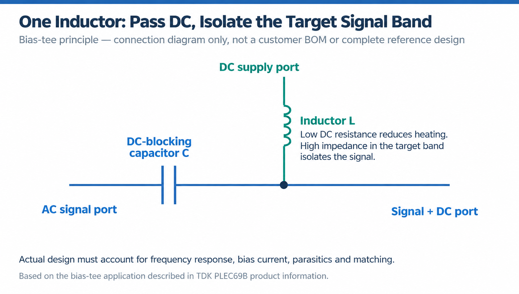
Figure 4. Bias-tee principle, not a specific customer circuit or complete reference design.
4. Thin-film experience is entering different parts of AI systems
Together, the two applications clarify the investment's technical context. Processor designs seek shorter power paths within height constraints. Optical transceivers need inductance, low DC loss and appropriate frequency behavior in tiny packages. Both place demands on magnetic materials, conductor structures and manufacturing, but they optimize different outcomes.
TDK attributes PLEC69B performance to metallic magnetic materials and structural design. Its earnings presentation also explicitly connects HDD-head thin-film technology to inductors. These disclosures support interpreting the expansion as a reuse of established process capabilities in AI-related components. Public information does not, however, quantify a cost, yield or gross-margin advantage.
The reported ¥40 billion plan therefore does not point to a single “AI inductor” market represented by one part number. On the processor side, value rests on power layout and loss. On the optical-transceiver side, it rests on electrical behavior under DC bias. A shared process can serve two different sets of circuit constraints and product-evaluation criteria.
This article is based on public information. Product specifications and supply developments remain subject to the manufacturer's latest disclosures.