
It is tempting to assume that moving an optical module from 1.6T to 3.2T doubles the operating frequency of every internal component. For DC-blocking and coupling capacitors in a high-speed channel, the pressure comes from two different directions: more lanes make component and pad placement denser, while higher per-lane rates require fresh analysis of insertion loss, reflections and characterization bandwidth.
A next-generation broadband capacitor therefore cannot be assessed by one maximum-frequency claim. Capacitance, package size, terminal structure and measured RF evidence all matter. Launchip's LXF223SA1K0092 combines 22 nF capacitance, an 01005 body, a two-terminal design and discrete typical insertion-loss values measured as high as 110 GHz.
1. From 1.6T to 3.2T: frequency is not the only challenge
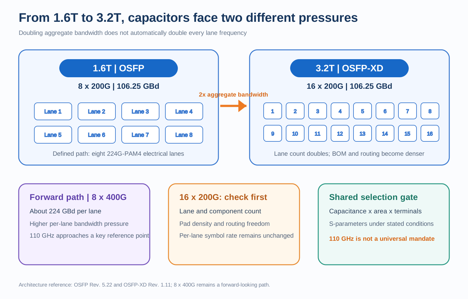
The OSFP specification defines a 1.6T AUI-8 interface using eight 224G-PAM4 electrical lanes, each carrying 200 Gbit/s at 106.25 GBd. A 3.2T AUI-16 path under OSFP-XD doubles the lane count to sixteen at the same per-lane rate. In that 16 x 200G architecture, aggregate bandwidth doubles primarily by adding lanes, components and routing density; the symbol rate of each lane does not change.
The industry is also developing a more forward-looking 8 x 400G architecture. A 400G lane is associated with roughly 224 GBd. Under a first-order Nyquist estimate, its critical baseband frequency is about 112 GHz, making 110 GHz a relevant characterization point for the individual channel.
For 1.6T and 16 x 200G designs, characterization to 110 GHz is mainly broadband margin. For an evolving 8 x 400G path, it becomes preparation for a much higher per-lane rate. It is not a universal mandatory capacitor requirement written into every 1.6T or 3.2T specification.
2. Why place 22 nF in an 01005 body?
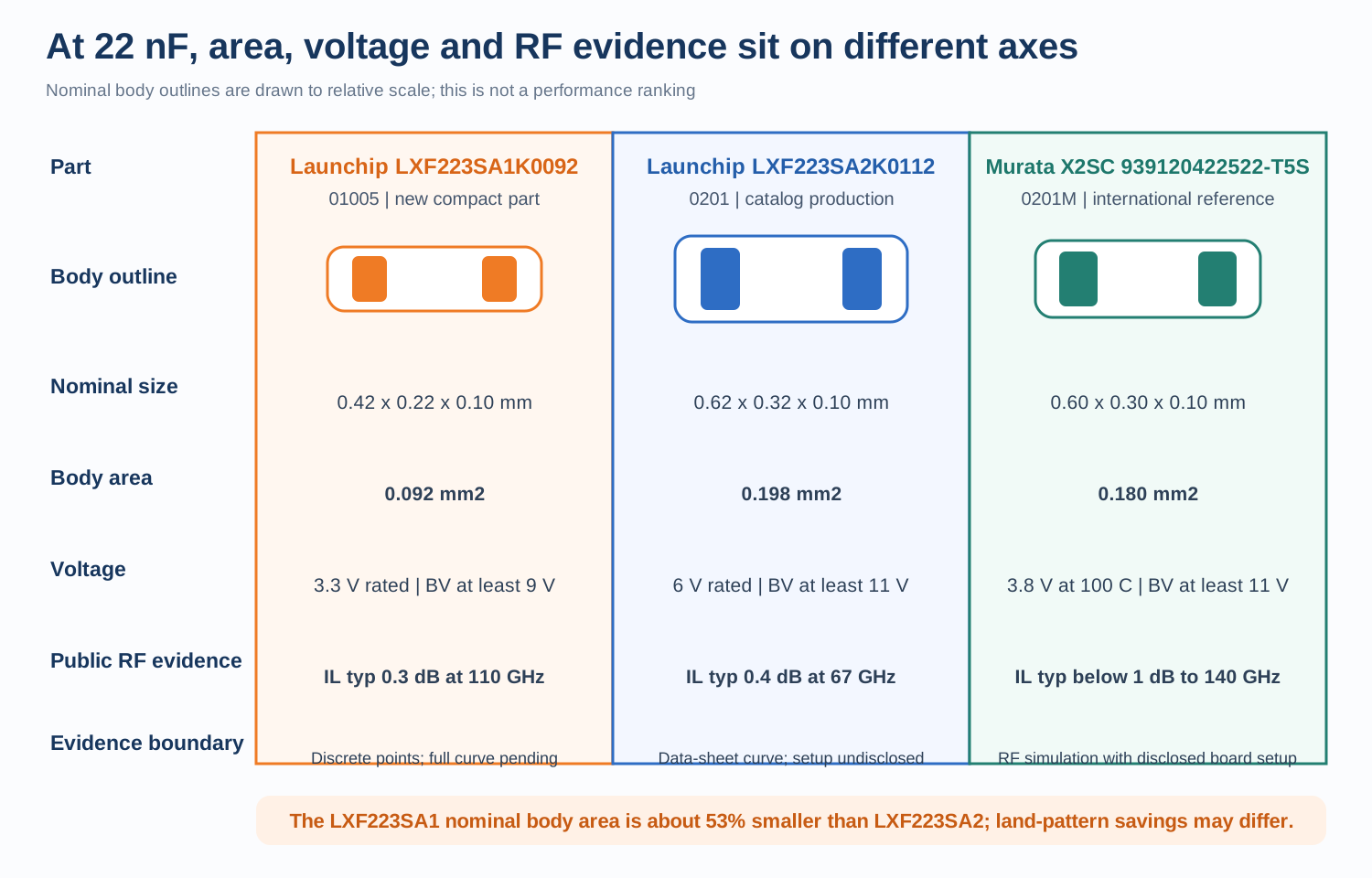
LXF223SA1K0092 is a two-terminal, 22 nF silicon capacitor measuring 0.42 x 0.22 x 0.10 mm. Typical thickness is 100 um and can be customized. Rated voltage is 3.3 VDC, breakdown voltage is at least 9 VDC, and the operating-temperature range is -55 to 150 degrees C. The 9 V value is a breakdown rating, not the rated operating voltage.
Launchip's earlier LXF223SA2K0112 provides the same capacitance in a 0.62 x 0.32 x 0.10 mm body. The nominal body area of the new device is about 53.4% smaller. That does not mean the land pattern or total board area shrinks by exactly the same amount, but in a dense sixteen-lane module it can create more room for pads, traces and adjacent components.
At 25 degrees C, the specification lists typical insertion loss of 0.10 dB at 20 GHz, 0.15 dB at 40 GHz, 0.25 dB at 67 GHz and 0.30 dB at 110 GHz. Typical return loss at 110 GHz is at least 13 dB. The 0.30 dB figure is a typical discrete measurement, not a guaranteed limit across every sample, temperature and bias. A complete S-parameter curve is still needed. The published points can support early evaluation but cannot replace a full Touchstone file or system simulation.
3. Products advertised around 110 GHz do not all solve the same job
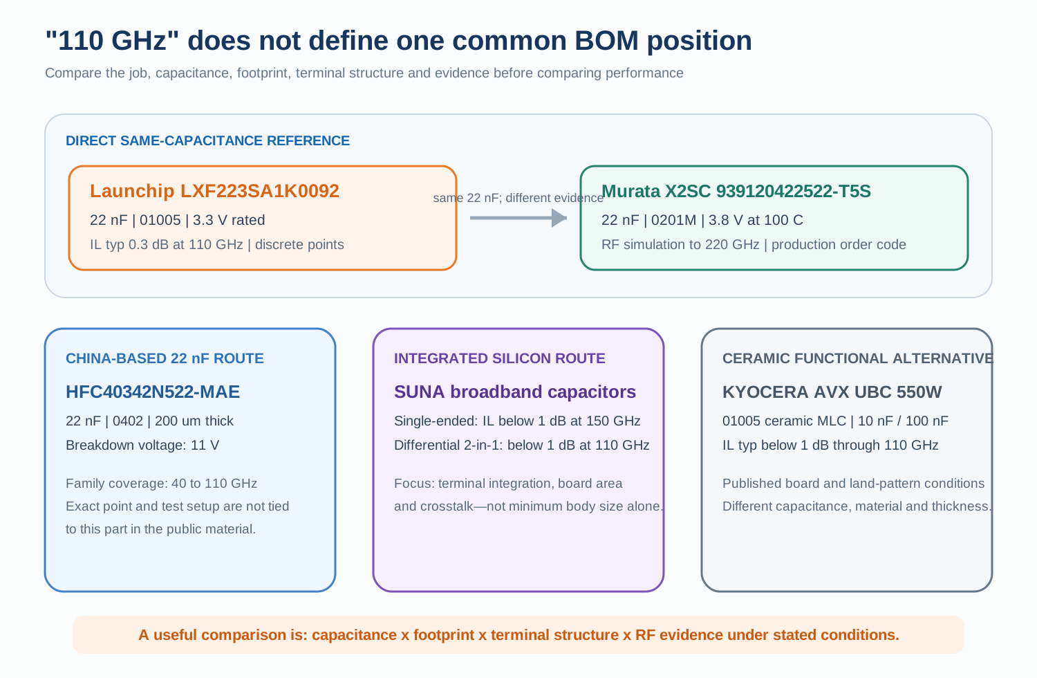
Murata's IPDiA X2SC 939120422522-T5S is another 22 nF silicon capacitor. It uses a 0201M body measuring 0.60 x 0.30 x 0.10 mm. Murata publishes simulated data to 220 GHz using a 10 mil quartz CPW in a 50 ohm environment, and the T5 ordering code supports production delivery. Murata's strengths include a mature RF model, disclosed test structure and established ordering system. Launchip differentiates by placing 22 nF in a smaller 01005 body.
China-based suppliers are also entering the segment. HFC40342N522-MAE is a 22 nF device in 0402 with 200 um thickness and an 11 V breakdown rating. Its HFC4 family is described for 40 to 110 GHz operation, but the public high-frequency statement is not tied to a specific test point and setup for this exact part, so it cannot be compared directly with Launchip's published insertion-loss values.
SUNA offers both single-ended and differential broadband silicon capacitors. Its public material lists single-ended insertion loss below 1 dB at 150 GHz and an integrated two-in-one differential device below 1 dB at 110 GHz. The design objective is terminal integration, board-area reduction and lower crosstalk rather than minimum body size alone.
Ceramic devices remain relevant. KYOCERA AVX UBC 550W103M and 550W104M are 01005 ceramic MLCs with 10 nF and 100 nF capacitance. The manufacturer specifies typical insertion loss below 1 dB through 110 GHz on a 5 mil Rogers RO3003 board with the recommended land pattern in a 50 ohm setup. This shows that 110 GHz operation is not unique to silicon, although capacitance, thickness and material behavior differ from Launchip's 22 nF device.
Skyworks' frequently cited SC family covers roughly 0.8 to 1000 pF and frequencies up to 26 GHz. A discontinuation notice was issued in May 2026. It is useful as a reference for an earlier MIS-silicon-capacitor generation, not as a mainstream competitor for the current 110 GHz design space.
4. Launchip's advantage is not the 110 GHz label by itself
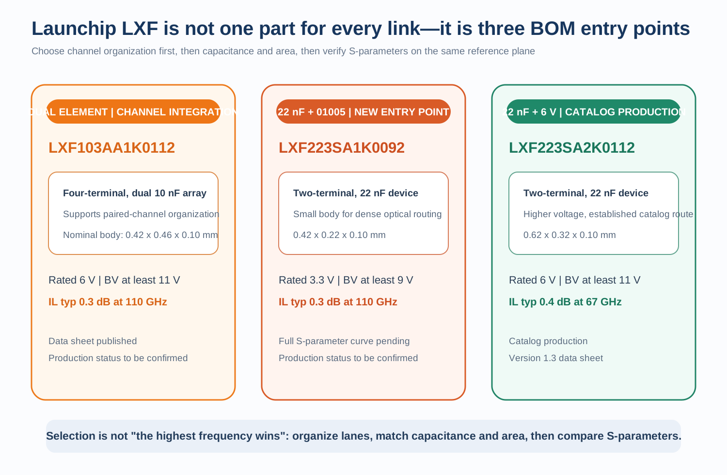
Launchip's own portfolio clarifies the role of the new part. LXF103AA1K0112 is a 10 nF, four-terminal dual-element array for channel integration. LXF223SA1K0092 combines 22 nF, an 01005 body and discrete values through 110 GHz. LXF223SA2K0112 provides 22 nF at 6 V rated voltage, at least 11 V breakdown and a complete 67 GHz S-parameter curve; it was included in the production catalog in May 2026.
These are not simply three performance tiers. They address different engineering priorities: channel integration, extreme miniaturization, voltage margin and production maturity. Compared with samples promoted only by a frequency band, Launchip has frozen capacitance, package, terminal arrangement and voltage into standard part numbers. Compared with established international vendors, it still needs broader public S-parameter data and a more mature volume-ordering record.
That combination—a strong package-size advantage with RF evidence still being completed—is a more useful description of the competitive position than a slogan claiming that a China-developed capacitor has "reached 110 GHz."
Conclusion: 3.2T creates more than a wider link
In the established 1.6T 8 x 200G route, 110 GHz is primarily a characterization and design-margin point. In a 3.2T 16 x 200G route, lane count and BOM density rise first. For the evolving 8 x 400G route, individual-channel bandwidth becomes the central problem.
Launchip's new device addresses both density and bandwidth evidence: 22 nF in 01005 responds to placement pressure, while discrete data to 110 GHz supports broadband evaluation. A data sheet alone cannot prove adoption in a 1.6T or 3.2T customer BOM, but it gives engineers a concrete component to qualify.
Disclaimer: This article is based on manufacturer public information and material supplied by Launchip. It is for industry discussion only and is not a procurement or part recommendation. Confirm parameters, product status and application suitability with the latest manufacturer documents and project validation.
