
A striking claim is circulating through the supply chain: a DRAM shortage has supposedly left TSMC holding about $1 billion worth of Apple 2 nm chips that cannot proceed to packaging. It is a dramatic headline, but it needs an immediate caveat. Neither Apple nor TSMC has disclosed such a $1 billion inventory, and no independently verifiable public data supports that exact figure. A more accurate description is that, if LPDDR does not arrive in step with the packaging plan, some N2 wafers, known-good dies, or work in process could remain upstream of final packaging. That is not the same as finished chips waiting only for an enclosure.
The rumor resonates because it captures one of the advanced-packaging era's sharpest contradictions: an expensive logic die made on the most advanced process can genuinely be held up by comparatively inexpensive mobile memory. The 2 nm node may set the performance ceiling, while LPDDR sets the minimum achievable production volume.
1. The $1 Billion Figure May Be Wrong, but a 10%-20% Pull-In Reduction Matters More
The market is currently prone to mixing together three separate issues: supply-chain expectations that Apple's next-generation A20/A20 Pro will use TSMC N2, reports of a new WMCM package, and the shortage of LPDDR. The A20 naming, actual specifications, and scope of any WMCM adoption have not been announced by Apple. It is also too early to treat the base and Pro models as confirmed users of the same packaging route.
More useful than the claim of a $1 billion pile-up is another supply-chain estimate: LPDDR constraints could leave Apple's actual early pull-ins of A20 devices from the second half of 2026 through the first quarter of 2027 some 10%-20% below the original target. Part of that gap could also reflect overbooking by Apple at an earlier stage. TrendForce's estimate for the second quarter of 2026 is more direct: average LPDDR5X contract prices could rise 78%-83% quarter over quarter. This is no longer merely a matter of higher memory prices; even buyers willing to pay may not receive sufficient volume on schedule.
TSMC N2 itself, by contrast, has moved beyond presentation slides. TSMC has confirmed that N2 entered high-volume manufacturing in the fourth quarter of 2025 and would continue ramping through 2026. That is what makes the situation notable: the most advanced wafer process can advance on schedule while the complete device is still constrained by material synchronization in the packaging bill of materials. TSMC's official financial results do show an unusual signal. Inventory days increased from 80 to 87 in the second quarter of 2026, up 11 days year over year, and TSMC explicitly attributed the increase primarily to the N2 production ramp. Total inventory rose by NT$74.08 billion quarter over quarter, while N2 contributed 3% of wafer revenue for the first time. These figures establish that N2 inventory and production were ramping rapidly. They do not establish that $1 billion of that inventory belonged to Apple, or that all of the increase resulted from a DRAM shortage. The claim that "$1 billion of A20 Pro devices are waiting for packaging" should therefore still be treated as supply-chain reporting, not as a conclusion from TSMC's financial statements.
2. The 2 nm Process Is Not Stalled; Memory Exposes WMCM's Weak Link
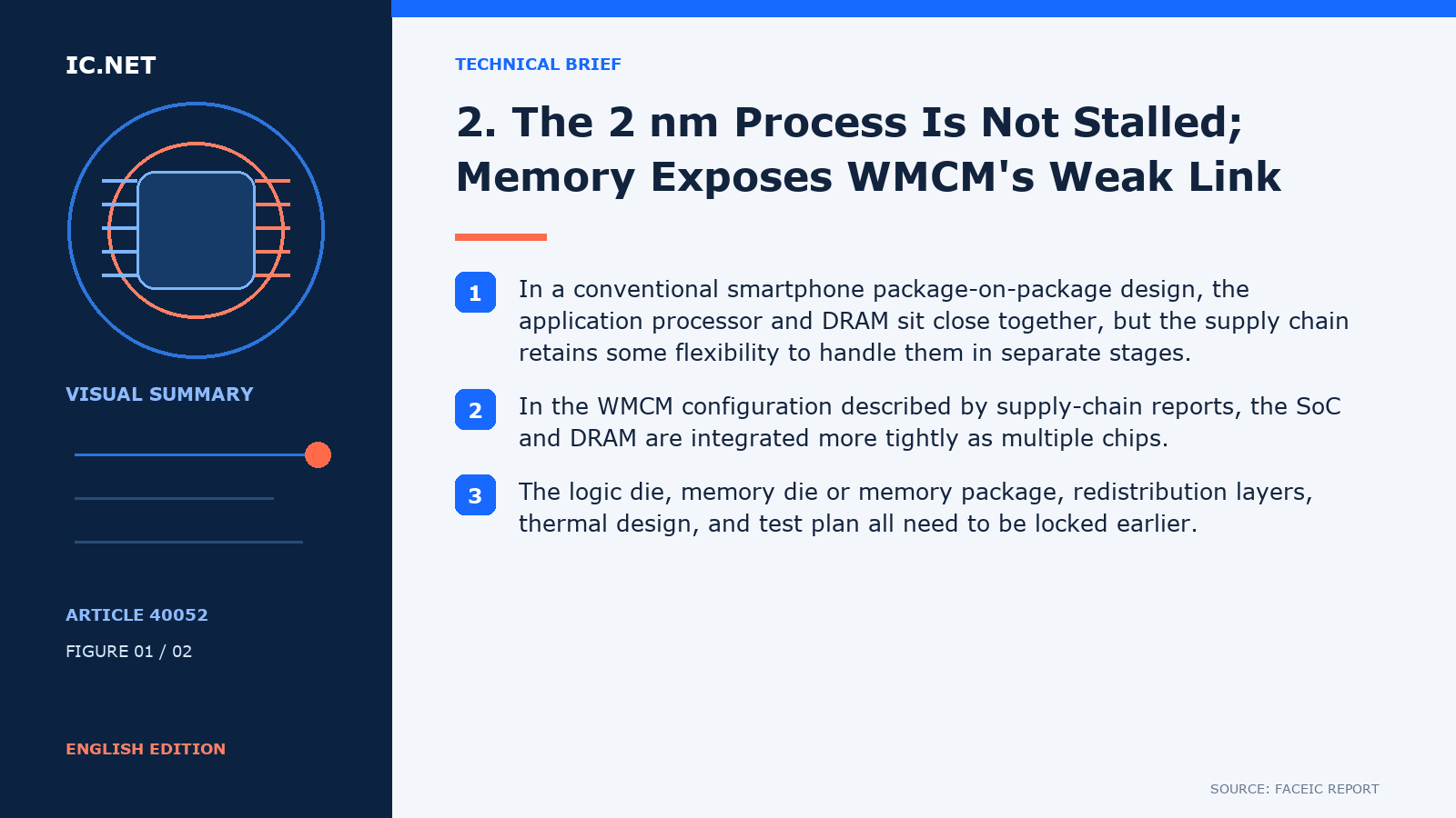
In a conventional smartphone package-on-package design, the application processor and DRAM sit close together, but the supply chain retains some flexibility to handle them in separate stages. In the WMCM configuration described by supply-chain reports, the SoC and DRAM are integrated more tightly as multiple chips. The logic die, memory die or memory package, redistribution layers, thermal design, and test plan all need to be locked earlier. Potential gains include shorter signal paths, a smaller package, and better thermal design. The cost is that a supply chain in which each party could previously deliver separately now has to meet the same deadline.
The bill-of-materials path can be simplified as follows: N2 wafer fabrication -> wafer test and known-good die -> LPDDR at the required capacity, speed, and power bin -> WMCM assembly -> final package test -> smartphone motherboard. If LPDDR falls behind in capacity allocation, lot consistency, or qualification timing, expensive N2 dies can become work in process waiting for material. At that point, whether and when the package can be assembled matters more than whether the logic die has already passed test.
3. Apple Does Not Need Just Any DRAM; It Needs the Device Qualified to Package with A20
Why not simply change suppliers? That sounds attractive in ordinary purchasing, but for a highly customized smartphone package it is about as optimistic as suggesting a different charger. Apple does not need an arbitrary component labeled LPDDR5X. It needs a device that matches the required capacity combination, speed grade, voltage and power, controller training, die dimensions and bump scheme, thermal behavior, yield, and long-term availability.
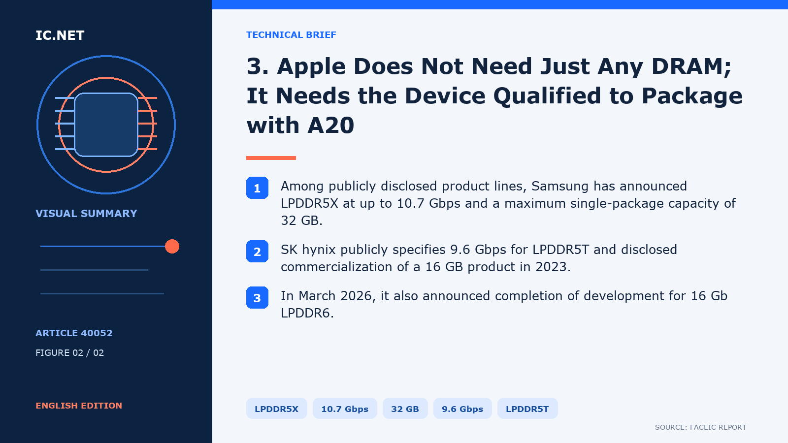
Among publicly disclosed product lines, Samsung has announced LPDDR5X at up to 10.7 Gbps and a maximum single-package capacity of 32 GB. SK hynix publicly specifies 9.6 Gbps for LPDDR5T and disclosed commercialization of a 16 GB product in 2023. In March 2026, it also announced completion of development for 16 Gb LPDDR6. However, "supply in the second half" remains an official plan and should not be reported prematurely as volume shipments.
Micron has publicly specified its 1-gamma LPDDR5X at up to 10.7 Gbps in a 16 GB configuration, claiming as much as 20% lower power consumption than its 1-beta generation. Its public catalog also lists LPDDR5X devices such as MT62F512M32D1DS-023RFWT, a 16 Gb, 8,533 MT/s, 315-ball component. That demonstrates the capability of a standard product; it does not show that the part is actually used with A20.
In China, CXMT has publicly listed LPDDR5X in 12 Gb and 16 Gb densities. Its 8,533 Mbps and 9,600 Mbps products entered mass production in May 2025, while the 10,667 Mbps product was described in October 2025 as being sampled to customers. CXMT therefore has a product line capable of competing in flagship mobile memory. But "a product exists," "Apple is testing it," "it has passed qualification," and "it has entered the A20 supply BOM" are four entirely different states. No specific Samsung, SK hynix, Micron, or CXMT part number for A20 has been disclosed in a way that can be independently verified.
4. Advanced Packaging Makes the BOM Interdependent: Lower-Cost Parts Can Hold Up Expensive Wafers
This is the part of the $1 billion rumor that deserves serious discussion. In a conventional BOM model, the main processor is the lead component, memory is secondary, and packaging is a finishing step. In WMCM, SiP, and other tightly integrated multichip designs, all three become part of the same product event. A delay in any one item can pull other high-value materials into inventory and can create disputes over rematching, retesting, down-binning, or scrap liability.
Even if a large volume of unpackaged die eventually accumulates, it would still be wrong to call it "$1 billion of TSMC inventory" without knowing the contracts and accounting treatment. The public does not know who prepays for the wafers, when ownership of known-good die transfers, whether the memory is customer-supplied or purchased by the packaging provider, or which party bears the cost of a delay. Physical custody at TSMC does not necessarily mean financial ownership by TSMC.
The lesson for procurement and hardware teams is direct: do not treat DRAM as a standard part to be quoted only two months before mass production. Projects using PoP, SiP, MCM, or WMCM should lock memory density, speed, and package form together with the main processor. Controller training, thermal and power testing, yield validation, and lot qualification should be completed for at least two sources. Contracts should also define capacity allocation, die preparation, rematching, and scrap liability. Otherwise, a small saving in memory unit price may not cover the financing and production-line cost of leaving a lot of N2 die idle for several weeks.
Conclusion: 2 nm Gets the Spotlight, but LPDDR May Control the Gate
The assertion that "TSMC has accumulated $1 billion of Apple 2 nm chips" remains an unverified market claim and should not be presented as established fact. The industrial tension it highlights is nevertheless real. Once logic, memory, and packaging share one production cadence, scarcity is no longer determined only by the process node. It is determined by whichever material is last to pass qualification and arrive on time.
TSMC's ability to manufacture N2 does not guarantee that Apple can ship A20 on its original schedule. The most dangerous component in a future BOM may not be the most expensive one, but the one that completes qualification last.
Disclaimer: This article is for industry discussion only and does not constitute investment, procurement, or part-selection advice. Supply relationships not confirmed by the companies involved are treated as reports or estimates.